
High-Z Semiconductors for h-keV Direct X-Ray Imaging
Project #: 22-082 | Year 1 of 2
Charles Leak,a Luke Hovey,a Tanya Atencio,a Daniel Dzenitis,b Anthony Botelloc
aNevada National Security Site, Los Alamos Operations (LAO); bNevada National Security Site, Livermore Operations; cNevada National Security Site, Special Technologies Laboratory
Executive Summary
Semiconductor ionizing-radiation detectors with high atomic numbers (high-Z) are being investigated to directly image x-rays on the order of 100 keV (h-keV) for use in flash radiography. In year one, unoptimized CdZnTe was used to measure an x-ray flash with commercial off-the-shelf (COTS) components, simulations were run to predict the physical limit of spatial resolution, and a sensor testbed for evaluating semiconductor sensor performance was designed and manufactured.
Description
Ionizing-radiation sensors made from semiconductors with high atomic numbers (having high electron density, thus high photon cross sections) are an alternative to scintillators in many applications which provide greater sensitivity, energy/dose resolution, and image resolution (e.g.- CdZnTe as a gamma-ray imaging spectrometer). Flash radiographs in the nuclear security enterprise are often captured using a scintillator and a silicon sensor array, which is insensitive to x rays because of its low absorption cross section. This project seeks to prototype and evaluate the advantage of an imager using a sensor array made of a high-Z semiconductor instead of silicon, which may provide the benefits listed above, perhaps at the expense of interframe time and signal linearity.
The primary materials of interest are CdTe and CdZnTe (CZT), but less mature materials such as TlBr and halide perovskites are of interest and may be evaluated in year two. First, an unpixellated thick CZT crystal was tested using COTS NIM module components to measure x-ray flashes from the linear accelerator (LINAC) at LAO. This thick CZT crystal was designed for use as a gamma-ray spectrometer; it is not optimal for x radiography (prone to polarization at high doses, only a single imaging pixel, etc.). Nonetheless, x-ray flashes were consistently detected, though pulse height and pulse integral variance and linearity measurements were inconclusive. Next, design and manufacturing of a customized testbed capable of amplifying signals from a pixelated semiconductor sensor began and pixelated CdTe and CZT sensors were purchased. A first iteration was completed and manufactured during year one by the coauthors hereof. Coupling a high-Z semiconductor to a modified Kraken Readout Integrated Circuit (ROIC) to evaluate the compatibility of existing custom NNSS electronics to this application was originally in the scope as well, but this evaluation may not be feasible due to timeline shifts caused by supply chain interruptions.
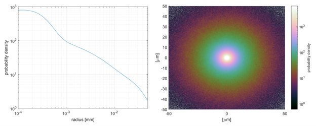
Geant4 Monte Carlo simulations were also run to estimate the spatial distribution of electron-hole pairs freed in CdTe from a pencil beam of bremsstrahlung off of a molybdenum target with an endpoint of 300 keV, shown in figure 1. This provides the first physical limit to spatial resolution of the proposed imager to a plausible x-ray source for mid-soft x-radiography. The limit is exceedingly small: the full width at half maximum (FWHM) was 0.8 μm, while the FWHM point-spread function for the light emitted from an identical crystal made of LYSO (Lutetium-yttrium oxyorthosilicate) under the same conditions was simulated to be 2.2 mm. This 0.8-μm FWHM does not include electron/hole diffusion nor electron/hole transport under laterally perturbed electric fields, which are generally negligible at small dose rates but may be significant in the dose rates seen in flash radiography. Incorportation of these physics will require other codes and will be considered in year two if significant experimental deviations are observed.
Conclusion
In year one, an unoptimized CZT crystal was used to measure an x-ray flash with COTS components, simulations were run to predict the physical limit of spatial resolution, and a sensor testbed for evaluating semiconductor sensor performance was designed and manufactured. The primary goals for year two are to measure signal variance and linearity, spatial point-spread function, and reset time with the new testbed and procured sensors. If the hardware is available, the compatibility between a Kraken ROIC and procured sensor will be investigated.
Mission Benefit
The testbed produced by this project introduced a tool by which to evaluate high-Z semiconductors for use in several applications in stockpile stewardship and global security. The new knowledge gained in year one is not significant, but the knowledge to be gained in year two with this testbed will determine feasibility of a new x-ray imaging technology which could provide greater sensitivity, signal resolution, and spatial resolution to flash radiography, especially in the energy range of hundreds of keV, directly improving future experimental data.
This work was done by Mission Support and Test Services, LLC, under Contract No. DE-NA0003624 with the U.S. Department of Energy. DOE/NV/03624–XXXX.
Return to Radiographic Systems Imaging and Analysis
Go to SDRD Annual Report Index
Return to SDRD Homepage