High-Z Semiconductors for h-keV Direct X-Ray Imaging
Project # 23-088 | Year 2 of 2
Charles Leaka, Kevin Thomasb, Daniel Dzenitisa, Luke Hoveya, Tanya Atencioa
aLos Alamos Operations (LAO), bRemoting Sensing Lab-Nellis (RSLN)
This work was done by Mission Support and Test Services, LLC, under Contract No. DE-NA0003624 with the U.S. Department of Energy, the NNSA Office of Defense Programs, and supported by the Site-Directed Research and Development Program. DOE/NV/03624–1935.
Abstract
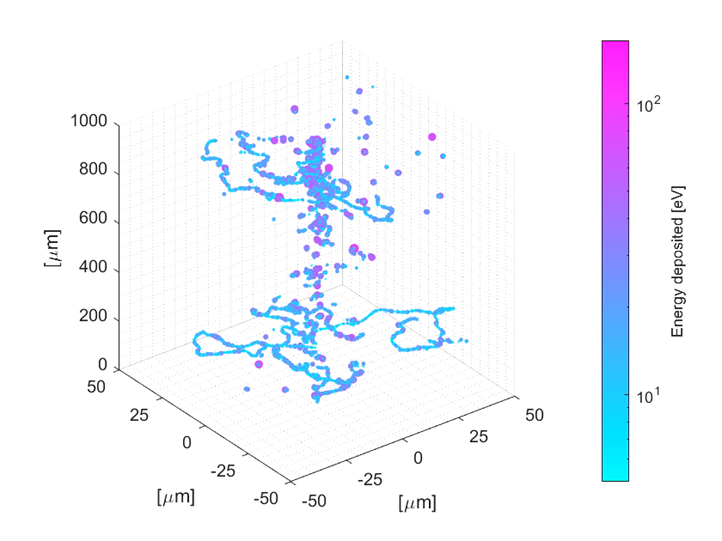
The goal of this project was to develop a prototype x-ray camera using a semiconductor with high atomic number instead of a scintillator imaged with a lens onto a silicon photodiode array. The x-ray energies of interest were on the order of 100 keV. A flexible testbed was constructed to evaluate semiconductor response to flash-flood x-ray irradiation. and initial results from flashflood irradiating pixelated semiconductor detectors using a linear accelerator were recorded. CdTe responded linearly over the tested 1-6 µR of 75-keV-endpoint bremsstrahlung; CdZnTe sample showed material defects likely caused by vendor; CsPbBr3 shattered during assembly but responded well to Cs-137 gamma irradiation. Simulation and calculations from first principles predicted twenty times better signal-to-noise ratio and nearly three thousand times smaller point-spread function full-width at half-max than currently used scintillator systems. Procurement delays retarded progress of testbed fabrication, preventing further testing, and programmatic rescheduling prevented coupling of semiconductors to modified Kraken readout integrated circuit. While no radiographs were recorded during this project, the hardware to record radiographs was designed, procured, fabricated, and tested. This hardware can also be used to measure semiconductor material properties via alpha and gamma irradiation. Next steps should include recording radiographs at different doses and interframe times, iterating hardware designs, and expanding to more semiconductor samples.
Background
Radiography in the nuclear security enterprise is generally accomplished using a flash x-ray source, a scintillator, and a visible-imaging camera. A scintillator is required because the visible-imaging camera is primarily a silicon photodiode array, which is insensitive to x rays of energy greater than a few dozen keV. X-rays that pass through the object of interest excite the scintillator, which scintillates upon deexcitation. Scintillation photons are collected using an optical relay and directed onto a camera sensitive to their wavelength. Features in the object of interest with high x-ray attenuation cross sections will cast x-ray shadows, which do not allow scintillation. The contrast between brightly scintillating regions of the scintillator and dark regions caused by object features reveals object information. Significant causes of loss of this information include optical scattering within the scintillator and poor collection efficiency by the optical relay. The purpose of this investigation was to replace the scintillator and silicon photodiode array with a semiconductor detector array having high detection efficiency for x rays around 100 keV. This removes the mentioned causes of information loss. Several semiconductors with high atomic number meet the criteria and are used for gamma-ray spectroscopy and medical imaging.
Technical Approach
First, a thick (1-cm3) cadmium zinc telluride, (CdZnTe) cube with planar anode and cathode was connected to an off-the-shelf (OTS) nuclear-instrumentation-module preamplifier and high voltage power supply (HVPS), and its response to flashes of bremsstrahlung with 1 MeV endpoint produced by the linear accelerator (linac) at Los Alamos Operations was recorded using an oscilloscope. Next, a testbed was designed, manufactured, and iterated. The testbed was composed of a printed circuit board (PCB), enclosure, and off-the-shelf components that enable measurement of the response of a pixelated semiconductor detector under ionizing irradiation. The PCB routes signal and power to and between the electrodes of a semiconductor detector (up to sixteen grounded electrodes and one biased electrode), charge-sensitive amplifiers, and an oscilloscope. The PCB allows variable coupling between the electrodes and amplifiers to accommodate large radiation responses; it allows simultaneous amplifier calibration while the detector is installed, and it allows reconfiguration without soldering. The enclosure blocks visible light and electromagnetic interference while passing signal and power through BNC and SHV type cable connectors; it has thin windows to minimize x-ray attenuation; it allows the PCB height to be adjusted to maximize radiation flux, and it has an accessory that allows a collimated alpha source to be mounted inside the enclosure above the source and rastered to probe spatially-dependent detector response for uncoated detectors. Two iterations of the enclosure and three iterations of the PCB were manufactured. Two versions of the final PCB iteration were designed and manufactured: one accommodating a 16-pixel footprint, and one accommodating a 64-pixel footprint with switching that allows one quarter of the 64 pixels to be read at a time. Additionally, a carrier assembly was designed and manufactured to mount one unbonded 64-pixel crystal. Two cadmium telluride (CdTe) (16 pixels), one CdZnTe (64 pixels), and one cesium lead bromide (CsPbBr3) perovskite (64 pixels, unbonded) detector were tested by Cs-137 gamma flood irradiation, and all but the CsPbBr3 were tested by flood irradiating with 75-keV-endpoint bremsstrahlung flashes produced by the linac. The CsPbBr3 shattered during installation in the carrier assembly. Linac irradiation was repeated at two distances for each detector. Average linac dose per flash was recorded using three pocket ionization chambers. Only seven pixels were measured at any time due to limited oscilloscope channels.
Results and Technical Accomplishments
The initial test with a CdZnTe cube demonstrated proof of concept by producing unsaturated waveforms with consistent shape but with large variance in amplitude; some variance was explained by beam current variance, so the dose per flash likely varied significantly. A flexible testbed was designed and manufactured that can probe detector properties and record radiographs with pixelated semiconductors. Using this testbed and irradiating with the linac, all three detectors responded linearly within the uncertainty of the independent dose measurement over the range of about 1 µR per flash to about 6 µR per flash. Cs-137 gamma irradiation revealed some high-impedance connections to pixels of the CdZnTe likely caused by manufacturing errors, and it exhibited promising performance of the largest chunk of CsPbBr3 despite shattering.
Conclusions and Path Forward
While no radiographs were recorded during this project, the hardware to record radiographs was designed, procured, fabricated, and tested. This hardware can also be used to measure semiconductor material properties via alpha and gamma irradiation. All three materials tested may be appropriate for use as flash x radiographic cameras. Next steps should include recording radiographs at different doses and interframe times, iterating hardware designs, and expanding to more semiconductor samples. Samples should vary across vendor (Acrorad, Actinia, Brimrose, Kromek, Redlen, RMD, and research groups), dimensions (thickness, pixel size), material (Cadmium Manganese Telluride (CdMnTe), Cadmium zinc telluride selenide (CdZnTeSe), high-flux CdZnTe, Thallium bromide (TlBr), wide bandgap methylammonium lead bromide (MAPbBr3), etc.), and electrode (ohmic or Schottky of various metals). More detailed testing with one material should inform sample selection (rise-time too slow, polarization present, leakage current too high, etc.). Operating bias and post-processing methods can be varied. Hardware can be changed to optimize dynamic range of detector. Readout using the nascent Continuous Imager should be investigated. Eventually, charge transport physics may be used to extract some spectral radiographic information, allowing for discernment of object elemental composition.