
Solid-State Spectrographic Camera for HED and Pyrometry Applications
Project #: 22-064 | Year 1 of 3
Amy Lewis,a Liam Claus,b Matthew Dayton,b Mike Jones,a Kevin O’Flarity,a Ivan Pegram,a Marcos Sanchezb
aNevada National Security Site; bAdvanced hCMOS Systems
Executive Summary
High-speed, nanosecond-scale, time-resolved radiance and pyrometry type measurements are essential to characterize advanced high energy density (HED) tests at the “Z-pinch” Pulsed Power Facility at Sandia National Laboratories (SNL) and the National Ignition Facility (NIF). Streak cameras suffer from poor detector efficiencies, variation in temporal resolution from shot to shot, and limited spectral range and overall sensitivity. A solid-state solution will provide a reliable, cost effective option with improved performance. The proposed solid-state spectrographic camera will incorporate a complementary metal oxide semiconductor (CMOS) sensor with a novel shutter distribution architecture to create an imager with ~100 ps resolution. A prototype design will be submitted to the SNL Microsystems Engineering, Science and Applications (MESA) foundry facility as a ride-along to reduce cost and realize a camera in three years.
Description
This high-speed, solid-state streak camera concept utilizes a standard two-dimensional focal plane array (FPA) architecture with a global electronic shutter. Standard FPAs collect spatial information in both the X and Y dimensions using an M rows × N columns array of pixels. This concept substitutes the spatial information in the X direction for temporal data, thus realizing an FPA that captures N, 1D images (of M rows of pixels). In this concept, an externally triggered, high-speed global shutter is generated, replicated, and then distributed to every row in the pixel array simultaneously, starting at the leftmost column of the array (column0). Every column of the pixel array contains a delay element that will delay each subsequent column by a programmed delay time. Therefore, each column captures a 1D image (of M rows) of spatial information while delaying the subsequent column shutter (image) by a delta-T on the order of 100–150 ps.
A time-varying input signal of photons is dispersed evenly across the image plane of the sensor using a cylindrical optic. A trigger synchronous to the experiment is issued to the FPA, and the image capture sequence begins. A rolling shutter propagates across the image plane, capturing linear images of the input signal starting at T0 and ending at TN. Readout of the sensor pixel array is performed, and M, 1XN images of the time-varying input signal are collected. Consistent input impedance on every pixel is enabled by each pixel having a single signal connection to a corresponding photodiode via three-dimensional interconnect. The scalable architecture is limited to the size of the two-dimensional FPA.
In the first year, the team developed a detailed camera architecture, which will enable a proof‐of‐concept design. The readout integrated circuit (ROIC) and detector design will be completed, targeting the SNL CMOS7 350nm process. The team has modeled the ROIC, detector, and system to predict performance under various input conditions and stimuli. Kathy Opachich, Hanna Shelton, and Minta Akin have provided feedback for initial use case considerations.
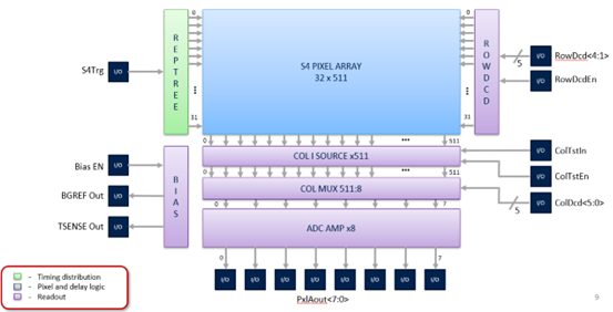
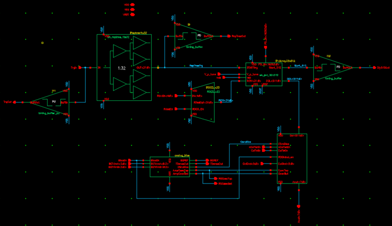
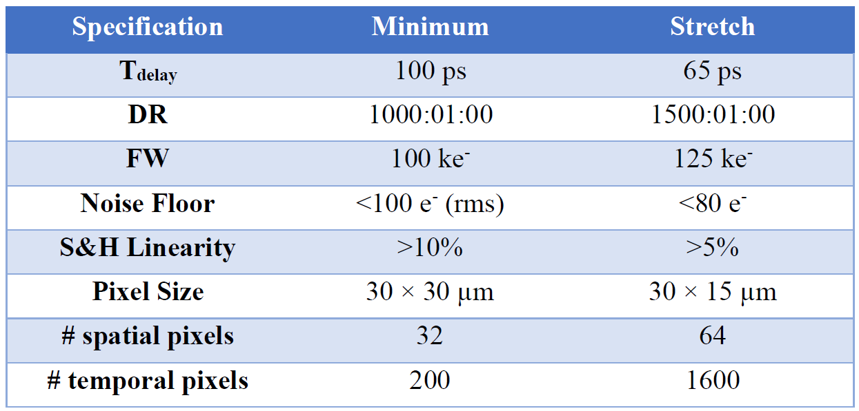
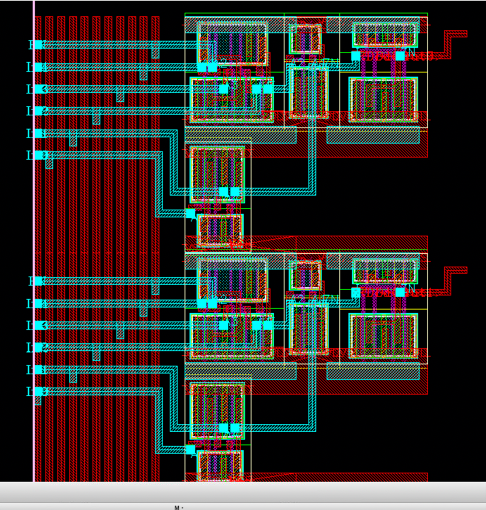
In Fiscal Year (FY) 2022, the ROIC schematic, layout, and parasitic extraction was completed. The team held preliminary and critical design reviews. The settled design specifications are shown in Table 1. The camera architecture was fully developed (Figure 1). The initial pixel has been laid out and has been simulated with full parasitic extraction. The S4 core schematic was finalized (Figure 2). Pixel test circuitry has been conceived to allow electrical testing of ROIC performance prior to the lengthy hybridization process.
The CMOS7 based delay cell was designed and optimized for speed. Schematic based design yielded an 80-ps minimum delay, limited by the CMOS7 technology itself. Layout was performed and simulations conducted, including full parasitic extraction, and yielded a 148-ps minimum delay. Typical layout parasitics reduce performance in CMOS7 by roughly a factor of 2, so this falls within expectations. Extensive parasitic extracted simulations were performed, including process mismatch and noise modeling, to verify timing distribution accuracy and sample-to-sample variation in the single picosecond range. Power supply voltage boosting was simulated to achieve a 125-ps minimum delay with a 4.0-V power supply. Investigations were performed to verify that large pixel array power/ground distribution was adequate while temperature simulations were conducted to bound performance across temperature variation. An on-chip temperature sensor was implemented to allow calibration for temperature. Sample and hold linearity sweeps across mismatch and noise were also conducted to verify linearity performance across dynamic range.
Table 1. Design Specifications
Conclusion
As shown in Figure 3, the design of the ROIC is complete and optimization nearing completion. The team anticipates that the design will be submitted to the foundry in the third quarter of FY 2023. The ROIC and detector will be fabricated and the FPA packaging defined while hybridization occurs. A camera test bench for the FPA will be designed. The final year’s effort will package the FPA and test it in a benchtop camera assembly.
Mission Benefit
A solid-state spectrographic camera capability would benefit many programmatic mission priorities in the following areas: HE driven ejecta temperature measurements for melt equation of state (EOS) of ejecta or bulk materials in dynamic shock tests to inform physics models; HE and detonator performance tests; and EOS for IHE tests or high-temperature pyrometry on gas gun tests. Dynamic high-temperature measurements currently with traditional streak camera systems are also a critical diagnostic at Z, Omega, and NIF in the HED program.
Streak cameras have been workhorses in the weapons program for underground testing and subcritical experiments, as well as for university research. Very few flexible solid-state solutions exist for the wide variety of streak camera experiments. If successful, this camera design will provide a significant opportunity for the NNSS to provide a state-of-the-art diagnostic system tailored to HED experiments.
Publications, Technology Abstracts, Presentations/Posters
A tech abstract will be filed when the design is submitted to the foundry (expected in the 3rd quarter of FY 2023).
This work was done by Mission Support and Test Services, LLC, under Contract No. DE-NA0003624 with the U.S. Department of Energy. DOE/NV/03624–1615.
Return to Radiographic Systems Imaging and Analysis
Go to SDRD Annual Report Index
Return to SDRD Homepage